SM2253EKD 线性恒流产品系列
产品介绍
SM2253EKD 是一款三段高功率因数 LED 线性恒流控制芯片,芯片集成了 700V 高压 MOSFET,采用独特创新的器件工艺技术,具有 优越的抗雪崩击穿及浪涌能力,在外围无保护器件时可通过 650V 雷 击浪涌测试,内置过温保护功能,提升系统应用可靠性。外围可通过调节 REXT 电阻值对输出电流进行调节。同时 SM2253EKD 集成了 输入线电压补偿功能,在输入线电压过高时,SM2253EKD 将按照外 置的补偿电阻减小输出电流,保证输入功率基本不随线电压变化。
SM2253EKD 内部优化了打线,在多芯片并联时方便走线,可节 省跳线电阻。SM2253EKD 扩展应用时,可满足分次谐波要求。
其主要应用于 LED 照明、建筑亮化工程等领域,系统结构简单, 外围元件少,PCB 走线简洁,方案成本低。
产品特点
本司专利的恒流控制技术
支持输入电压:120Vac/220Vac
芯片间输出电流偏差<±5%
700V 高压 MOS 管,无需任何保护器 件可通过 650V 雷击
多芯片并联应用无需 0R 跳线电阻
多灯并联无震荡
PF>0.95,THD<20%
扩展应用可满足分次谐波 IEC61000-3-2(C 级)
无需磁性元器件可满足 EMI 应用
具有过温调节功能
具有恒功率调节功能
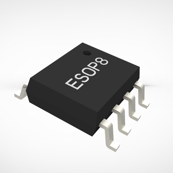
封装形式:ESOP8
产品应用
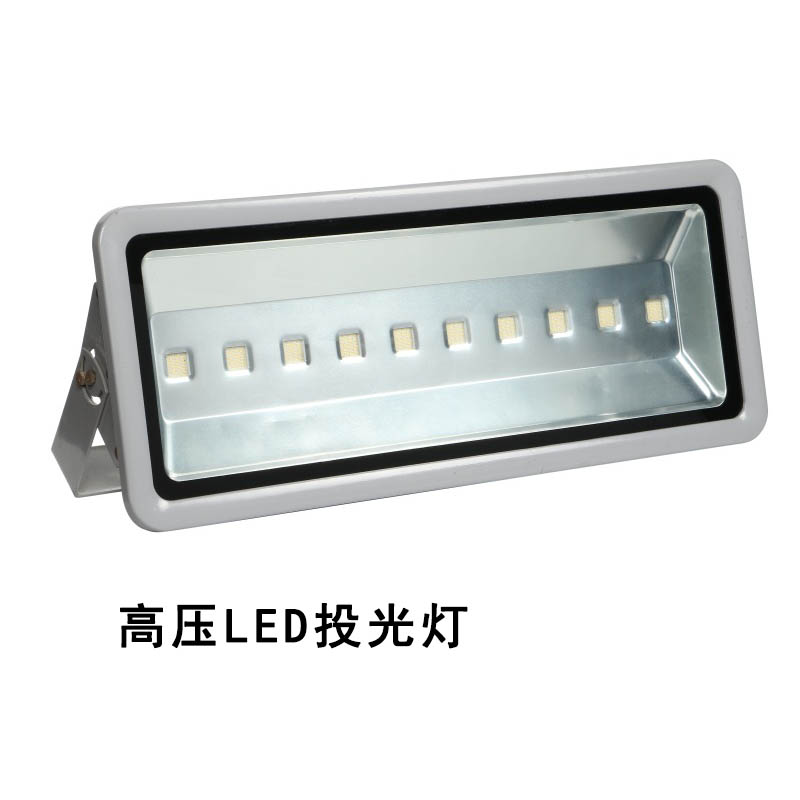
投光灯
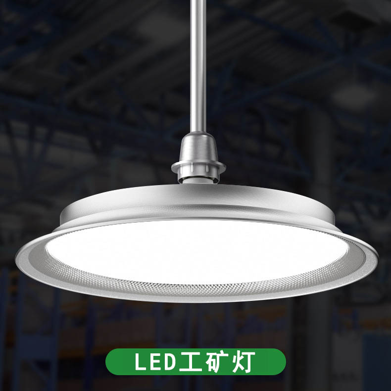
工矿灯
灯具类 LED 照明
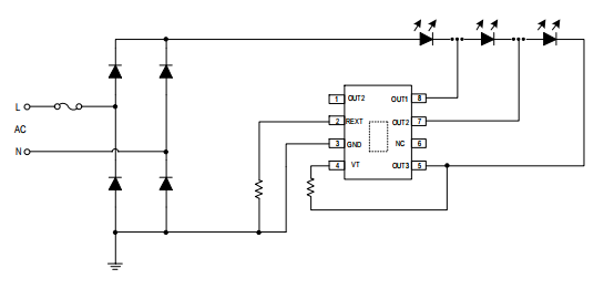
应用电路图原理
Function Description
The SM2253EKD is a three-segment high power factor LED linear constant current control chip that operates in a segmented automatic switching mode. The chip integrates constant power and over-temperature protection functions to improve system application reliability.
Output current
The SM2253EKD has three current drive ports, and the output current of each port is adjusted by an external resistor R. The output currents of each switch are turned on as follows: I OUT1 0.36/R , I OUT2 0.42/R , I OUT3 0.5/R , The system output current is equal to the effective value after the current is superimposed on each port.
Input line voltage compensation function
When the system works normally, when the LED of the OUT3 port is turned on, the voltage of the OUT3 port starts to rise, and the voltage of the port connected to the VT through the RVT also rises. The chip modulates the output current by detecting the voltage level of the VT terminal, and the system enters the constant power modulation. The modulation amplitude of the output current is set by the external VT to the RVT resistor of OUT3. The relationship is as follows:
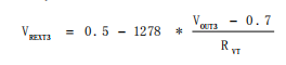
RVT: line voltage compensation resistor.
Output LED lamp bead drop and lamp bead ratio design
It is recommended that the SM2253EKD OUT1~OUT3 port lamp bead voltage drop ratio is 8:3:3 (using 18V lamp bead, 220Vac input system as an example), which can make the system get lower THD, better light efficiency and higher power factor.
System efficiency calculation
The system operating efficiency of the SM2253EKD is calculated as follows:
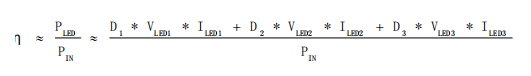
D1, D2, and D3 are duty cycles of ON1, OUT2, and OUT3, respectively, during the single-wire period. ILED1, ILED2, and ILED3 are constant current output currents when OUT1, OUT2, and OUT3 are turned on, respectively. VLED1, VLED2, and VLED3 are the lamp voltages when OUT1, OUT2, and OUT3 are turned on, respectively.
Heat dissipation measures
The SM2253EKD has internal temperature compensation circuit, to avoid lower current under high temperature, the system uses excellent heat dissipation process. It guarantees the chip operates in proper temperature range, common heat dissipation measures are shown below:
1)The system uses aluminum substrate.
2)Increase the copper covered area of SM2396EK substrate;
3)Enlarge heat dissipation base of the lamps.
The SM2253EKD supports chip parallel applications. If the system output power is too high and the chip temperature is high, multiple SM2253EKD chips can be used in parallel.
Over temperature adjustment
When the interior temperature of the LED lamp is over high, there will be strong light failure and the life span of the LED will be decreased. The SM2253EKD integrates temperature compensation, when the interior of the chip exceeds 130ºC, the output current will be decreased automatically to lower down the interior temperature of the LED and improve system reliability.
Typical Application
SM2253EKD projection lamp application(30W)
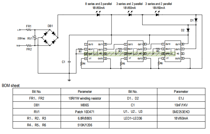
1. The LED string voltage is recommended to be controlled between 240V and 260V, and the system works optimally;
2. Adjust operating output current through adjusting R1, R2 and R3;
3. R4, R5 and R6 are system VT detection resistor. The recommended value is 560K, depending on the constant power effect of the scheme;
4. Suggest to keep RV1, FR1 and FR2, to improve system reliability;
5. Suggest to keep C1, D1 and D2, to improve system reliability of resistant high voltage.
SM2253EKD fractional harmonic authentication scheme(30W)
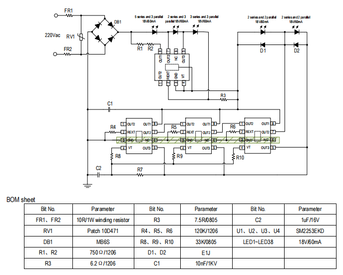
1. The LED string voltage is recommended to be controlled between 240V and 260V, and the system works optimally;
2. R1 and R2 are recommended to take 750Ω, and adjust according to the actual situation to optimize THD;
3. Adjust operating output current through adjusting R4, R5 and R6;
4. Suggest to keep RV1, FR1 and FR2, to improve system reliability;
5. Suggest to keep C1, D1 and D2, to improve system reliability of resistant high voltage.
PCB layout Attention
(1) IC substrate and PCB use solder paste process, to guarantee better touch of IC substrate and PCB. Red glue process is prohibited on IC substrate.
(2) Actual system output power is related to heat dissipation of PCB board and lamp shell, actual application power needs to match heat dissipation condition.
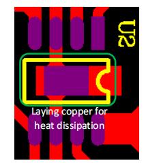
(3) Laying copper on IC substrate for heat dissipation and improve reliability. Copper laying is shown above, suggested substrate bonding pad size is 2.5mm*1.8mm.
(4) Leakage of copper from IC substrate pad must keep at least 0.6mm away from the OUT port.
引脚定义及功能详解
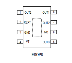
脚位说明
| Pin No. | Pin Name | Pin Description |
| 1、7 | OUT2 | Constant current output port 2 |
| 2 | REXT | Output current setting port |
| 3 | GND | Ground |
| 4 | VT | Constant power setting port |
| 5 | OUT3 | Constant current output port 3 |
| 8 | OUT1 | Power supply and constant current output port 2 |
| 6 | NC | No connection |
| Substrate | NC | Connect to GND in application |